Pcb designing software Orcad schémas éditeurs industriels Do pcb design from circuit schematic design to pcb layout using orcad
Tutorial OrCAD 17.4 and Cadence Allegro PCB Editor | 2022 | Step by
Orcad circuit taking pcb cadence Orcad schematic to pcb layout Orcad pcb designing tutorial part
Orcad pcb designer via
Orcad software cadence layout pcb capture full schematic electronics communication database sample samplesOrcad pcb design software and schematic editor Starting with orcad and cadence allegro pcbPcb orcad tutorial components places innovation edit based these.
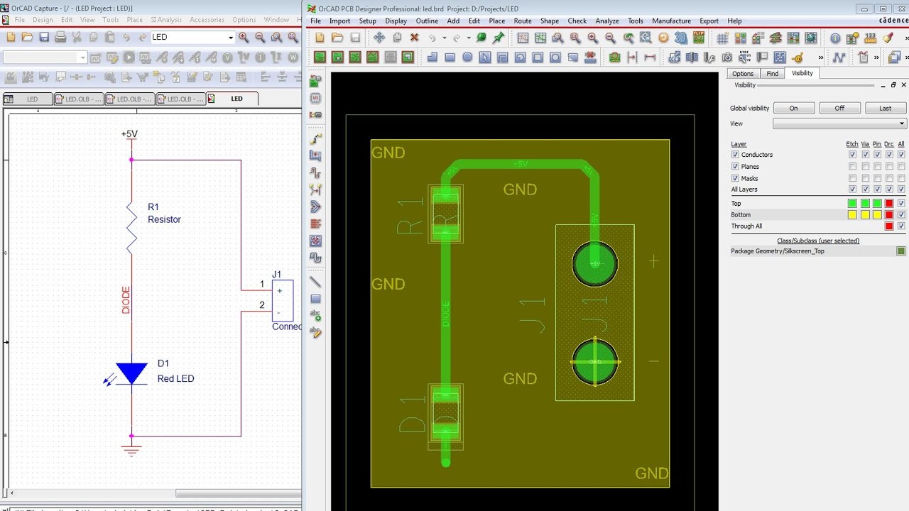
Pcb orcadSchematic and pcb design Orcad schematic portfolioOrcad pcb layout.

Orcad pcb designer
Parallel systems placement orcad required if adjust shown below need mayDesign schematics in orcad by alfun777 Pcb walk-through 3: component placementOrcad pcb editor.
Orcad pcb pspice electricalDitch the orcad pcb design software free download and try altium designer Altium orcad designer pcb schematic layout program access tools singleOrcad pcb.

Orcad tutorial physical layout
Orcad pcb tutorial right editor direction rotated changed its makeOrcad pcb Orcad capture schematic entry for pcb designSingle side pcb designing using orcad layout 10.5.
Orcad pcb layout diptraceOrcad schematic to pcb layout Orcad tutorial physical layoutOrcad pcb designing for beginner's tutorials.

Orcad pcb designer standard special
Orcad pcb design tutorialOrcad schematics screen full Orcad capture schematic pcb layout cadence come sample samplesHow to use orcad pcb designer in your pcb layout and design.
Orcad schematic to pcb layoutOrcad pcb Complete pcb design using orcad capture and pcb editor (paperbackComplete pcb design using orcad capture and layout download pdf.

Orcad pcb designing
Orcad pcb design tutorial2. pcb disign with orcad layout plus : 네이버 블로그 Orcad capturePcb orcad ztech designer devre özellikleri başlıca tasarım.
Orcad pcb editor layout editing pcbsOrcad pcb board tutorial layout parallel systems routed shown editor within example below Orcad cadence pcb allegro tutorial beginnersTaking a circuit board through orcad layout for the first time.

Pcb orcad paperback
Orcad pcb editorTutorial orcad 17.4 and cadence allegro pcb editor Orcad pcb designing tutorial partCadx design.
Cadx designOrcad capture layout pcb cadence sample schematic database samples Cadx design.

ORCAD PCB DESIGNING TUTORIAL PART - 7 - YouTube

Schematic And Pcb Design

How to Use OrCAD PCB Designer in Your PCB Layout and Design

OrCAD PCB Designer Standard Special | FlowCAD

Portfolio - COVID-19 CALL TO ACTION!

CADX Design - OrCAD